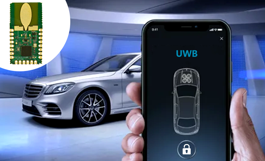
introduction
With the rapid development of wireless communication and Internet of Things technology, the need for positioning and ranging is becoming more and more urgent. Ultra-wideband (UWB) technology comes into being and becomes one of the effective solutions to this problem. UWB technology utilizes the large bandwidth and short pulse transmission characteristics of the spectrum, and has unique advantages in ranging and position positioning. This paper will introduce the design principle and optimization method of UWB chip in detail, aiming to help readers understand how to realize ultra-wideband ranging applications with high precision.

First, the working principle of UWB chip
UWB chip is the core component of UWB system, which contains the transmitter, receiver and modem and other functional modules. Its working principle can be simply summarized as the following steps:
1. Pulse transmission: The ultra-wideband ranging UWB chip transmits data by generating a series of short pulse signals. The bandwidth of these pulse signals is very wide, often reaching several hundred megahertz or more.
2. Propagation and reflection: the pulse signal will encounter the reflection of objects and the environment during transmission. These reflected signals are picked up and processed at the receiving end.
3. Reception and demodulation: After the UWB chip receives the transmitted and reflected signal, it uses a demodulator to convert it into a digital signal for subsequent processing and analysis.
4. Distance calculation: By calculating the propagation time delay and signal transmission speed, the distance of the object can be accurately measured. The ranging accuracy of UWB technology is usually between a few centimeters and a few millimeters.
Second, the key elements of UWB chip design
In order to achieve high precision ultra-wideband ranging, the design of UWB chips needs to consider the following key elements:
1. High bandwidth: The UWB chip needs to have enough band width to ensure that the signal can transmit more information and provide more accurate ranging results. Therefore, it is necessary to choose circuit elements and topology reasonably in chip design to meet the requirements of high bandwidth.
2. Low noise: Because the bandwidth of the UWB signal is very wide, noise suppression is very important for the chip design. The low noise design can improve the signal-to-noise ratio of UWB chip, thus enhancing the accuracy and reliability of ranging.
3. High-speed data sampling: Ultra-wideband ranging UWB chip needs to sample high-speed signals to obtain accurate time measurement. Therefore, it is necessary to select the appropriate sampling rate and sampling accuracy in the chip design to meet the needs of high-speed data sampling.
4. Low power consumption: Low power consumption is an important consideration in UWB applications. For mobile devices and low-power applications, the design of high-performance and low-power UWB chips is critical. In chip design, it is necessary to take a series of power optimization measures, such as power management and circuit optimization.
Third, UWB chip design optimization method
In order to achieve high-precision UWB ranging applications, the following are some UWB ranging UWB chip design optimization methods:
1. Bandwidth optimization: Choosing the right bandwidth is an important part of UWB chip design. The tradeoff between transmission distance and data rate should be considered in the design to determine the appropriate bandwidth range. By choosing filters, modems and other components properly, the bandwidth of the signal is optimized and no interference is ensured.
2. SNR optimization: Because UWB signals have high bandwidth characteristics, they are easily affected by noise. In the process of chip design, it is necessary to take measures to reduce the influence of noise on signal quality and ranging accuracy. For example, appropriate signal processing algorithms and noise reduction filters are introduced to improve the signal-to-noise ratio.
3. Clock synchronization optimization: In UWB system, accurate clock synchronization is crucial to ranging accuracy. In the chip design, it is necessary to consider the clock synchronization method and circuit design to ensure that the clock synchronization at the sending and receiving end is stable and accurate.
4. Power optimization: In mobile devices and low-power applications, reducing power consumption is a key design goal. The power consumption of UWB chip is optimized by optimizing power management, reducing circuit power consumption and adopting low-power sleep mode.
5. Rf circuit design: The design of RF circuit is crucial to the performance of UWB chip. Through reasonable selection of RF circuit topology, matching network, power amplifier device, etc., the signal transmission and receiving process are optimized, and the accuracy and stability of ranging are improved.
6. High-speed data sampling: The UWB chip requires high-speed data sampling to achieve accurate time measurement. In the design, it is necessary to select the appropriate data converter and sampling rate, and consider clock synchronization and signal filtering to ensure accurate data sampling.
peroration
UWB chip design is the key to realize high precision ranging and positioning. By optimizing the bandwidth, signal-to-noise ratio, clock synchronization, power consumption, RF circuit design and high-speed data sampling of UWB chip, more accurate and reliable UWB ranging applications can be realized. In the future, with the continuous development of UWB technology and the expansion of application scenarios, the optimization of UWB chip design will continue to become an important research direction, bringing more possibilities to achieve a wider range of UWB applications.


